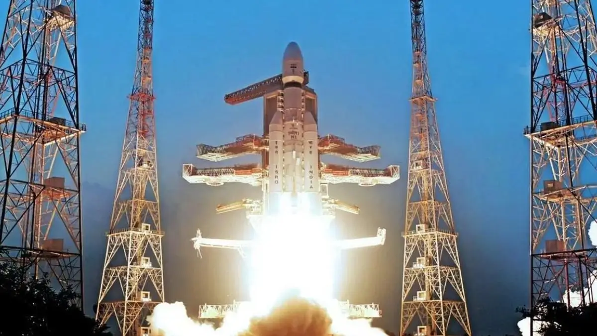








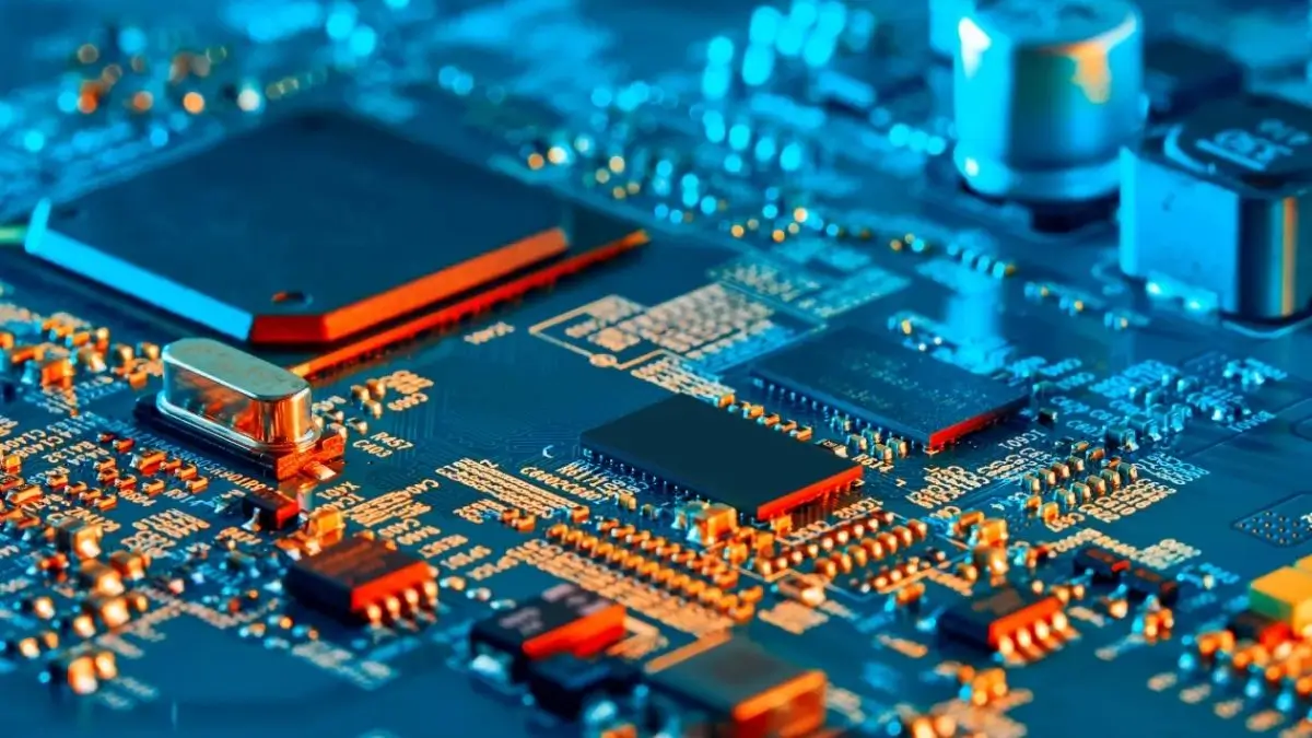
Semicon 2.0 semiconductor mission gets a ₹1,27,500 crore outlay to strengthen India’s chip design, fabrication, packaging, R&D, equipment and talent ecosystem.
Government Expands India’s Semiconductor Mission
The Government of India has notified Semicon 2.0, the next phase of the Semicon India Programme, with a fiscal outlay of ₹1,27,500 crore. The initiative is designed to strengthen India’s semiconductor ecosystem and move beyond chip manufacturing towards a complete value chain covering design, fabrication, packaging, equipment, materials, research and development, and skilled manpower.
Focus on Building a Complete Semiconductor Ecosystem
Semicon 2.0 is built around six strategic pillars: chip design, machines and materials, semiconductor fabrication facilities, ATMP/OSAT, research and development, and talent development. This broader approach is intended to reduce dependence on overseas supply chains and help India establish itself as a competitive global hub for semiconductor manufacturing and design.
Major Investment Boost for India’s Chip Industry
The semiconductor push is backed by substantial investment from both the government and private sector. By December 2025, 10 semiconductor projects with a combined investment of about ₹1.60 lakh crore had been approved across six states. These projects include silicon fabrication, silicon-carbide manufacturing, advanced and memory packaging, and specialised assembly and testing facilities.
Six Strategic Pillars of Semicon 2.0
The first pillar focuses on strengthening chip design, an area where India already possesses a large pool of engineering talent. The second covers domestic production of semiconductor machines and specialised materials. The third aims to establish additional semiconductor fabrication facilities, while the fourth seeks to expand ATMP and OSAT capabilities used for assembly, testing and packaging. The remaining pillars focus on advanced R&D and developing the skilled workforce required by the semiconductor industry.
Push for Semiconductor Research and Innovation
Research and development has become an important component of Semicon 2.0. Semiconductor technology requires continuous innovation because chip architectures, manufacturing processes and packaging technologies evolve rapidly. Greater domestic R&D capacity can help India develop indigenous technologies and strengthen its position in strategically important areas such as artificial intelligence, telecommunications, automotive electronics and defence technology.
Semiconductor Talent Development Gets Priority
Human resources are another major focus of the programme. India has already developed a significant semiconductor engineering talent base under the first phase. During the first phase, around 85,000 semiconductor engineers were trained, and the government has now set an additional target of developing one lakh semiconductor design engineers.
Importance for India’s Strategic and Economic Security
Semiconductors are essential components in smartphones, computers, automobiles, telecommunications equipment, defence systems, artificial intelligence infrastructure and many other modern technologies. Building domestic capabilities can therefore improve India’s supply-chain resilience and reduce vulnerability to disruptions in international semiconductor markets.
Semicon 2.0 and Atmanirbhar Bharat
The programme also supports the broader objective of Atmanirbhar Bharat, or self-reliant India. Instead of concentrating only on importing finished chips, the expanded programme seeks to develop capabilities across the semiconductor value chain. This can create opportunities for Indian companies, startups, research institutions and engineering professionals while encouraging foreign investment and technology partnerships.
Employment and Manufacturing Opportunities
The expansion of the semiconductor ecosystem is expected to create direct and indirect employment opportunities. According to current reporting on the programme, Semicon 2.0 could generate tens of thousands of direct jobs while also supporting wider employment through electronics manufacturing, logistics, engineering services, research and industrial supply chains.
Why Semicon 2.0 Matters for India’s Global Position
The semiconductor industry has become closely linked with economic competitiveness and national security. Countries across the world are attempting to strengthen domestic chip supply chains. By expanding support from fabrication to design, packaging, equipment, materials, R&D and talent, India is attempting to build a more integrated semiconductor ecosystem rather than relying on a single segment of the industry.
Exam Perspective: What Aspirants Should Remember
For government examinations, candidates should remember that Semicon 2.0 is the second phase of the Semicon India Programme, has a fiscal outlay of ₹1,27,500 crore, and is centred on six pillars: design, machines and materials, fabs, ATMP/OSAT, R&D and talent development. The first phase, Semicon 1.0, was launched with an outlay of ₹76,000 crore.

Why this News is Important
Semiconductor Self-Reliance
Semicon 2.0 is important because semiconductors are now a foundational technology for almost every modern economic and strategic sector. From smartphones and electric vehicles to artificial intelligence and defence systems, the availability of advanced chips directly affects technological capabilities. Strengthening domestic production can therefore contribute to India’s technological and economic resilience.
Strategic Supply-Chain Security
The global semiconductor industry is concentrated in a limited number of countries and regions. Disruptions caused by geopolitical tensions, natural disasters, trade restrictions or sudden changes in demand can affect chip availability worldwide. Developing domestic capabilities can help India diversify its sources and make critical supply chains more resilient.
Manufacturing and Investment
The programme is also significant from an economic perspective because it seeks to attract large-scale private investment into a high-technology manufacturing sector. Existing approved semiconductor projects have already represented around ₹1.60 lakh crore in investment, showing the scale of India’s emerging semiconductor ecosystem.
Employment and Skill Development
Semicon 2.0 places particular emphasis on talent development. The semiconductor industry requires specialised engineers, researchers, technicians and designers. The programme’s focus on developing semiconductor talent can therefore support high-skilled employment and strengthen India’s engineering and technology capabilities.
Relevance for Competitive Examinations
For aspirants preparing for UPSC, PCS, banking, railways, defence and other government examinations, the initiative is important because it connects multiple syllabus areas, including science and technology, manufacturing, economic development, strategic security, industrial policy, employment and Atmanirbhar Bharat. Questions may focus on the scheme’s financial outlay, implementing institution, six pillars and relationship with Semicon 1.0.
Historical Context: India’s Semiconductor Journey
Beginning with Semicon 1.0
India’s organised semiconductor manufacturing push received a major policy boost when the Union Cabinet approved the Semicon India Programme in December 2021. The programme carried an overall financial outlay of ₹76,000 crore and sought to establish a domestic semiconductor and display manufacturing ecosystem.
Establishment of the India Semiconductor Mission
The India Semiconductor Mission (ISM) was established as the institutional framework for implementing India’s semiconductor strategy. It plays a central role in evaluating and facilitating projects and developing an ecosystem spanning semiconductor manufacturing and design.
Expansion of Approved Projects
The first phase gradually resulted in major project approvals involving semiconductor fabrication, assembly, testing and packaging. By December 2025, 10 projects worth approximately ₹1.60 lakh crore had been approved across six states.
Transition to Semicon 2.0
Semicon 2.0 represents the next stage of this strategy. While the first phase concentrated significantly on establishing foundational manufacturing capacity, the second phase takes a broader ecosystem approach. It seeks to strengthen design, equipment, materials, fabrication, advanced packaging, R&D and human resources simultaneously.
From Manufacturing Capacity to Technology Ecosystem
The evolution from Semicon 1.0 to Semicon 2.0 reflects India’s larger ambition of becoming not merely a location for chip assembly or manufacturing but a participant across the semiconductor value chain. The government’s current strategy therefore combines manufacturing incentives with research, innovation, design capabilities and talent development.
Key Takeaways from Semicon 2.0
| S. No. | Key Takeaway |
|---|---|
| 1 | Semicon 2.0 is the second phase of the Semicon India Programme aimed at creating a robust and resilient semiconductor ecosystem in India. |
| 2 | The programme has a fiscal outlay of ₹1,27,500 crore. |
| 3 | Its six strategic pillars are chip design, machines and materials, fabs, ATMP/OSAT, R&D, and talent development. |
| 4 | The first phase, Semicon 1.0, was launched with an outlay of ₹76,000 crore to build India’s semiconductor and display manufacturing ecosystem. |
| 5 | By December 2025, 10 semiconductor projects worth about ₹1.60 lakh crore had been approved across six states, providing a foundation for the expanded semiconductor strategy. |
FAQs: Semicon 2.0
1. What is Semicon 2.0?
Semicon 2.0 is the next phase of India’s semiconductor development programme. It aims to build a comprehensive semiconductor ecosystem covering chip design, fabrication, packaging, equipment, materials, research and talent development.
2. What is the fiscal outlay of Semicon 2.0?
The fiscal outlay of Semicon 2.0 is ₹1,27,500 crore.
3. What was the outlay of the Semicon India Programme?
The original Semicon India Programme (Semicon 1.0) was approved with a financial outlay of ₹76,000 crore.
4. What are the six pillars of Semicon 2.0?
The six pillars are:
- Chip design
- Machines and materials
- Semiconductor fabrication facilities
- ATMP/OSAT
- Research and development
- Talent development
5. What is the India Semiconductor Mission?
The India Semiconductor Mission (ISM) is the institutional framework responsible for implementing India’s semiconductor strategy and supporting the development of the semiconductor ecosystem.
6. Why are semiconductors important for India?
Semiconductors are essential for smartphones, computers, automobiles, telecommunications, artificial intelligence, defence systems, industrial electronics and several other strategic sectors.
7. What does ATMP mean in the semiconductor industry?
ATMP stands for Assembly, Testing, Marking and Packaging. These are important stages in semiconductor manufacturing after fabrication.
8. What does OSAT stand for?
OSAT stands for Outsourced Semiconductor Assembly and Test. OSAT facilities perform important assembly, packaging and testing functions for semiconductor products.
9. How is Semicon 2.0 different from Semicon 1.0?
Semicon 1.0 primarily established the foundation for semiconductor and display manufacturing in India. Semicon 2.0 takes a broader ecosystem approach, covering design, fabs, equipment, materials, packaging, R&D and skilled talent.
10. Why is Semicon 2.0 important for government exams?
The initiative is relevant to Science and Technology, Economy, Manufacturing, Strategic Affairs and Government Policies. Aspirants should remember its ₹1,27,500-crore outlay, six pillars, and connection with India’s semiconductor self-reliance strategy.
Some Important Current Affairs Links